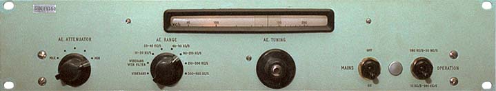
Racal RA137 LF Converter.
Detailed Tecnical Information.
Version 1.00
RA137 Circuit Diagram: GIF 163K
RA137 Top View: GIF 221K
RA137 Underside View: 239K
RA137 Technical Specification:
Freq Range: 10 to 980KHz.
Nominal Input Impedance: 75Ω
Aerial attenuator ranges: 0, 10, 20, 30, 40dB.
Preselector ranges: Wideband, Wideband with 500KHz LPF, 10-20KHz,
20-40KHz, 40-90KHz, 90-210KHz, 210-500KHz, 500-980KHz.
Sensitivity, A1, 3KHz Bandwidth: 1μV for 15dB s/n.
Sensitivity, A2 30% mod, 3KHz bandwidth: 3μV for 15dB s/n.
Image Rejection (tuned input): better than 60dB.
Spurious responses: less than 1dB above noise.
Mains Input: 100-130V, 200-250V (adjustable in 5V steps), 45-65Hz,
approx 11W.
HT Supply: 220V DC nominal.
1MHz Reference Input: Greater than 2V RMS, high impedance.
RF Output: 2 - 3MHz (Input freq + 2MHz).
AVC Input Control Range: 0V (max gain), -25V (min gain).
19" Rack mounting, panel height 2U (3.5" max.).
Electrical Differences between RA137 and RA137B
|
Component |
Function |
RA137 (UK) |
RA137B (N America) |
|
V1 |
RF Amp. |
EF93 (CV454) |
6BA6 (EF93) |
|
V2 |
Freq. doubler |
EF91 (CV138) |
6AU6 (EF94) |
|
V3 |
Bal. Mix. |
6F33 (CV2209) |
6AS6 |
|
V4 |
Bal. Mix |
6F33 (CV2209) |
6AS6 |
|
V5 |
Volt. Stab. |
150C2 (CV1832) |
0A2 (150C2) |
|
V6 |
RF Out. |
EF91 (CV138) |
6AU6 (EF94) |
|
|
|
|
|
|
R25 |
V3 grid 1. |
180Ω |
deleted |
|
R26 |
V3 grid 3 |
180Ω |
deleted |
|
R28 |
V3/V4 cath. |
82Ω |
33Ω |
|
R30 |
V4 grid 3 |
180Ω |
deleted |
|
R32 |
V4 grid 1 |
180Ω |
deleted |
|
R38 |
V6 Cath. |
82Ω |
39Ω |
|
R39 |
V6 grid 2 |
4.7KΩ |
15KΩ |
North American versions have an SO239 aerial connector and 75Ω
BNC sockets for 1MHz in and RF out. British versions have obsolete
NSF and Burndep connectors, which can be replaced without affecting
the alignment of the unit.
500KHz LPF.
THe RA137 is equipped with a 500KHz LPF which is in circuit on
ranges 10 - 500KHz and wideband with filter. This is to reduce
interference from strong medium-wave stations. Rejection frequencies
of the filter are at 560 and 680KHz, but should rejection be required
at specific frequencies close to these (within ±5%), the
appropriate cores can be re-adjusted. L2//C4 and L4//C6 reject
680KHz, and L3//C5 rejects 560KHz.
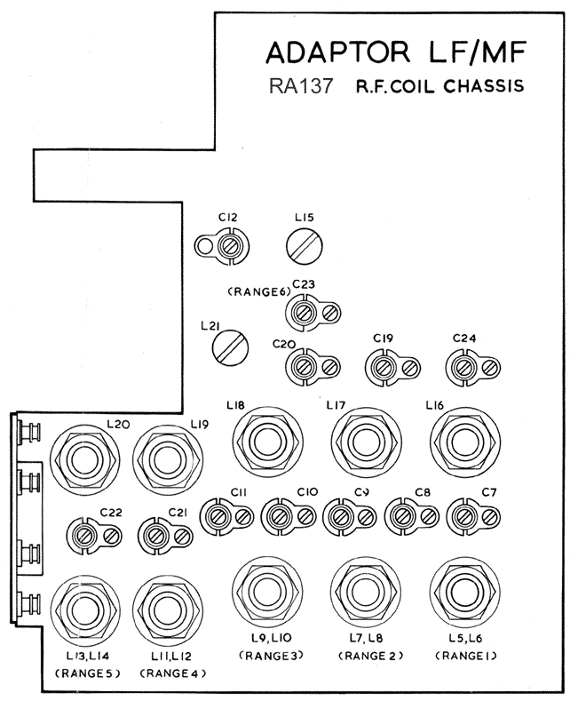
Preselector Tracking Adjustments.
The preselector uses a two-point tracking scheme, with the
adjustment points at the band edges. Tune the interpolation receiver
to the LF end of the band and adjust the coils for maximum signal
with the preselector dial set to the receiving frequency. Then
tune to the HF end of the band and likewise adjust the trimmer
capacitors for maximum signal. Repeat the procedure over and over
again until the required adjustments become insignificant.
|
Range / KHz |
LF end |
HF end |
|
Set Point |
Adjust |
Set Point |
Adjust |
|
10-20 |
10KHz |
L5*, L16 |
20KHz |
C7*, C24 |
|
20-40 |
20KHz |
L7, L17 |
40KHz |
C8, C19 |
|
40-90 |
40KHz |
L9, L18 |
90KHz |
C9, C20 |
|
90-210 |
90KHz |
L11, L19 |
210KHz |
C10, C21 |
|
210-500 |
210KHz |
L13, L20 |
500KHz |
C11, C22 |
|
500-980 |
500KHz |
L15, L21 |
980KHz |
C12, C23 |
*Adjustment of L5 and C7 is very flat and consequently not critical.
Adjustment locations:
1MHz LPF.
Image rejection is accomplished by feeding the output from the
RF amplifier (V1) through a low-pass filter consisting of three
constant K sections with m-derived end sections. R17 and R24 are
equal to the characteristic impedance of the filter. The filter
cut-off is at 980KHz.
To set up the LPF, apply a signal to the antenna socket with all
input filters and attenuators out of circuit. Measure the signal
arriving at V3 pin 1, with V3, V4, and V5 removed. To avoid overloading
the RF stage, keep the signal generator output below 800mV RMS.
Adjust L26 to obtain minimum output at 1030KHz. Adjust L22 to
obtain minimum output at 1080KHz. Apply a 100mV signal at 500KHz
and check that the signal at V3 pin 1 is not less than 800mV.
The frequency response from 10KHz to 980KHz should be within the
limits +1 and -3dB relative to the level at 500KHz. Adjust L23,
L24, and L25 as necessary to correct the response in the region
of 980KHz and ensure that there are no output responses above
1020KHz..
Harmonic generator (frequency doubler).
V2 is biased for non-linear operation. The output bandpass filter
is tuned to 2MHz, and has a bandwidth of 50KHz. An electrostatic
screen is placed between L33 and L34.
The 2MHz drive level at pin 6 of 6F33 V3 and V4 (pin 7 of 6AS6)
should be at least 0.5V RMS (ie, the 2MHz output accross the balanced
winding L34, when loaded by R27 + R29 should be greater than 1V
RMS.
Align the frequency doubler with its screening covers in place.
Check that there is ≥2V RMS of 1MHz drive at PL2. Measure the
doubler output at grid 3 of V3 (pin 6 if 6F33, Pin 7 if 6AS6).
Adjust L29, L30, and C50 in turn for maximum output.
Balanced Mixer.
British versions of the adapter use 6F33 mixer pentodes for V3
and V4. North American versions (RA137B) use 6AS6 mixer pentodes
and omit the grid-stopper resistors R25, R26, R30, R32. Mixer
pentodes, also called 'dual control' or 'short suppressor base'
pentodes, differ from normal pentodes in that grid 3 has a close
wire spacing and is internally connected to a diode (between grid
3 and the cathode) which prevents grid-current. The 6F33 and 6AS6
are not pin compatible (g2 and g3 connections are swapped) and
different cathode resistor values are used (see electrical differences
table above).
The balanced mixer has a broadband output. The anode load (L32//R31)
is broadly tuned to 2.7MHz, which is the logarithmic centre of
the 2 to 3 MHz output range. To measure the frequency response
of the stage, inject a signal into V3 grid 1 ((pin 1) with the
antenna disconnected, and measure the output across a 330Ω
terminating resistor connected across the RF output socket. Adjust
L32 for maximum output at 2.7MHz.
Mixer balance adjustment is by RV1 (front panel preset) and C52,
set by tuning the RA17 interpolation receiver to 2MHz (0 on the
red scale) and minimising the carrier level.
Back to LF
adapters Page.
Home | RA17
index | LF Adapters Page